Adhesion of Vacuum Deposited Films and Coatings. Part 4: Interface formation and its effects on adhesion

Author: Donald M. Mattox

The condensation/nucleation of depositing atoms (“adatoms”) on the surface is important in determining the adhesion/deadhesion at the interface or in the near-interface material [1,2]. The atoms nucleate on a surface by one of three modes as defined by E. Bauer in 1958 [3].

  1. Volmer-Weber (V-W) model. In the V-W model adatoms move over the surface and form isolated islands that grow three dimensionally before they join, possibly leaving voids at the interface. The nucleation may be random due to adatom collisions on the surface or may be associated with “preferential nucleation” sites. In some cases the poor bonding allows the liquid-like nuclei to move over the surface. This gives rise to the so called “island-channel-film” growth mode.
  2. Frank-van der Merwe (F-vdM) model – This model is also called the “layer-by-layer” growth model. In the F-vdM model adatoms form continuous layers on the surface with low numbers of adatoms as a result of a high nucleation density.
  3. Stranski-Krastanov (S-K) model – This model of growth is also called the “layer plus island” growth model. In S-K the first several monolayers of the adatoms that are condensed on the surface change the composition and/or structure of the surface. This changes the properties of surface to become less conducive to layer growth and more conducive to island growth (i.e. V-W type growth) which is favorable to some forms of nanotechnology that use isolated islands on a surface.

Bauer’s classification applies to epitaxial growth* of atomistically deposited films on a substrate, where diffusion at the interface is not desirable. For understanding film/substrate adhesion we need to add another nucleation mode where there is adatom reaction or mixing with the surface layer that makes the surface more conducive to high density nucleation and subsequent diffusion. If there is diffusion the reaction/mixing front may move laterally as well as normal to the surface.

* Epitaxy means the oriented growth of a crystal film on a crystalline substrate where the crystalline orientation of the film is determined by the orientations in the substrate surface. The term epitaxy comes from the Greek roots epi (ἐπί), meaning “above”, and taxis (τάξις), meaning “an ordered manner.” Epitaxial growth of single crystal films is important in the semiconductor industry.

As condensation continues, the interface between the film and substrate may or may not change due to interdiffusion and chemical reaction. The general types of interfacial regions are: 1) an abrupt transition of composition and properties, 2) A gradual transition of composition and properties (“graded interface”) over a few to many atomic layers, or 3) multiple interfaces by layering between the substrate and the coating. The layers may be different materials or one material with different properties.

Mattox characterized the types of interfaces formed during vacuum coating in 1965 [4,5] as 1) Monolayer-to-monolayer (abrupt), 2) mechanical interlocking (abrupt), 3) diffusion (alloying), 4) compound (diffusion with chemical reaction), and 5) “pseudodiffusion” (physically mixed). Types 3, 4 and 5 develop a layer of “interphase” interfacial material, which may determine the “practical” (apparent) adhesion of the coating to the substrate.

The monolayer-to-monolayer interface is characterized by an abrupt change from the film material to the substrate material in a distance comparable to the separation between atoms, with no diffusion between the film and substrate. Gold on carbon films, which was used for early transmission electron microscope (TEM) in situ studies of nucleation is an example of a non-reacting, abrupt type interface. Adhesion is due to low-value atom-to-atom bonding such as van der Waals bonding. The growth of the nuclei may exhibit a “dewetting” type of growth where the condensing adatoms try to avoid the nuclei-substrate interface and condense on the like-material of the nuclei (V-W nucleation) giving primarily growth normal to the surface.

The mechanical interlocking interface is characterized by interpenetration of the depositing atoms into the pores and roughness of the substrate to produce a “mechanical interlocking” “adhesion” as well as that from atom-to-atom bonding.

The diffusion interface requires solid solubility and the net movement of atoms from a region of high concentration to a region of lower concentration, usually at an elevated temperature. Some degree of solid solubility is necessary for diffusion. Diffusion may be substitutional between lattice sites or interstitial between the lattice sites. In substitutional diffusion the diffusing species may leave Kirkendall voids in the interfacial region due to differing diffusion rates (“Kirkendall Effect”). Diffusion from the substrate into the interfacial region affects the composition, properties, and structural phase of the “interphase” material. This may give a more easily fractured material. The diffusion rate may be enhanced along emerging grain boundaries and edge dislocations in the substrate. These actions tend to roughen the compositional boundaries and create interfacial mechanical interlocking which is conducive to improved adhesion.

A compound interphase material is formed when the diffusing material chemically reacts with the matrix material to form a compound. The strongest chemical bonds are the ionic bonds formed when one atomic species loses an electron to the other atomic species (e.g. oxides, nitrides). Metal-metal ionic compounds (“intermetallic compounds”) may be formed (e.g. UAl3 [6], AuAl2 {“purple plague”}). Elements that may either gain or lose electrons in a chemical reaction, such as aluminum, are called amphoteric elements. Compounds are generally more brittle than alloyed materials. The extent of the compound interface may be self-limiting if the interphase layer does not allow diffusion through the compound material formed (i.e. a “barrier layer”). A mixed diffusion-compound (“dispersed phase” or composite) interphase material may be formed if there is limited solubility of one material in the other.

The pseudodiffusion type interface is characterized by a gradient of composition that is not due to normal concentration-driven diffusion. The pseudodiffusion type interface may be generated is a variety of ways including: 1) high energy ion implantation (>5 keV) with gradually lowering of the incident ion energy), 2) low energy (<5 keV) ion implantation into the first few atomic layers of the near surface region (“subplantation”), 3) implantation of surface atoms into the near surface region by recoil from a bombarding particle (“recoil mixing”), 4) reaction with a gas or vapor to give a compound, composite or graded interface the composition of which may be controlled by the availability of the reactant gas/vapor (O,N), or 5) co-deposition of two or more condensable species to give a reacted, mixed, composite, layered or graded interfacial region the composition of which may be controlled by the relative flux of condensing species. The pseudodiffusion type interface does not require that there be solubility of the condensable materials.

The pseudodiffusion type of interface may be found in arc vapor deposition and high impulse power magnetron sputtering (HIPIMS) process technology where copious numbers of coating “self-ions” are generated in the vaporization process and are used to bombard the surface at high energies before and during the deposition.

Multi-layer graded interfaces are often used to “grade” from one material to another over a short distance [7]. For example in metallizing glass with gold, chromium may be used as an intermediate layer (“glue layer”) since the chromium is oxygen-active that adheres to the glass and has solid solubility to bond to the gold. The intermediate layer may also be formed by having a reactive gas available during a portion of the deposition of the intermediate layer. For example E. Hollar et al used a multi-layer graded interfacial region to metallize an oxide ceramic surface by sputter deposition [8]. The construct was: oxide / Nb:O / Nb / Nb:Ag / Ag. The resulting coating could be brazed with a Cu:Ag eutectic braze material (780oC; 72%Ag:28%Cu) to give a strong, vacuum tight seal.

Sputtering of the depositing film material during deposition may leave a coating that just consists of the interfacial compound material. The formation of platinum-silicide contacts to silicon is one application of this technique. Compound materials generally have a slower sputtering rate than do the elements.

Low nucleation density during film growth may leave pinholes and closed voids in the deposited film and fracturing due to film stress during growth may leave microcracks in the coating. This “through porosity” may affect adhesion by “pinhole corrosion” and interfacial corrosion. Adhesion failure by interfacial corrosion may be exacerbated by expansion of the corrosion products and “wedging” of the propagating crack by the corrosion products.

There are numerous ways that the composition, extent, morphology and properties of the interfacial region may change with subsequent processing, time, storage and/or use. The changes may degrade or improve the adhesion with time. This was first noted by P. Benjamin and C. Weaver in 1961 [9]. These possibilities should be taken into consideration when developing an adhesion test program and in the retention of archival samples.

Diffusion to or away from the interface may change the interface with time and affect the adhesion of the film. The principal diffusion paths are grain boundaries and dislocations. Periodic exposure to a reactive gas during deposition may reduce this diffusion by “plugging” these diffusion paths.

Early studies of the structure and morphology of vacuum deposited thin films were done with optical microscopy, electron diffraction and electron microscopy. The effect of off-normal adatom flux on the columnar morphology was recognized in 1953. With the advent of the scanning electron microscope (SEM) in 1965 (Cambridge Scientific Instrument Company – “Stereoscan”) [10] the columnar morphology could be more closely studied by fracture crossection and imaging the fracture surface. The SEM provided an analytical tool that allowed better studies on the growth morphology of sputter-deposited materials and the effects of concurrent bombardment on the growth [11].

In 1969 B.A. Movchan and A.V. Demchishin developed a “structure diagram” showing the relationship between the film morphology of “vacuum condensates” with atom deposition normal to the surface and the substrate deposition temperature (Tdep) normalized to the melting point of the material (Tmp) {i.e. (Tdep/Tmp)} [12]. This is called the “MD structure zone model” (MD-SZM).

In 1974 J. Thornton published a “structure-zone model,” (SZM) for sputter deposition where there was no deliberate bombardment during deposition [13,14]. This diagram came to be known as the “Thornton Diagram”. The Thornton Diagram illustrates the relationship between the deposit morphology, the deposition temperature, and the pressure in the sputtering chamber. The sputtering pressure determines the flux and energy of the reflected high-energy neutrals from the sputtering cathode, so the diagram also reflects the degree that the depositing material is bombarded by energetic neutral particles during low-pressure sputtering. Others further refined the structure zone model to incorporate more sputter deposition parameters. In 1981 the invention of the scanning tunneling microscope (STM) allowed the atomic-scale observation of surface features and nucleation phenomena.

It has long been known that film morphology can play a role in the optical properties of atomistically deposited films. It was not until 1950 that H. König and G. Helwig recognized that atomic-scale shadowing (“ballistic shadowing”) promoted the columnar morphology [15]. L. Holland pointed out the effect of vapor incidence on the morphology of aluminum deposited films in 1953 [16]. Deposition with an off-normal adatom flux gives columns that are inclined from the normal and face more toward the source of the atom flux. By using a low angle-of-incidence, rotation, and varying the angle-of-incidence (glancing angle deposition – GLAD), “sculpted films” may be grown.

No matter what the nucleation mode, atomistic deposition leads to a rough surface as the film thickens if the adatom surface mobility is low. Ballistic shadowing (“self-shadowing”) will lead to the development of a columnar morphology where each column adhers to the substrate but there may be poor adhesion of the columns to each other (fig. 10.5 in [17]).

Concurrent or periodic bombardment by energetic atomic-sized particles during deposition may be used to disrupt the columnar growth by “compaction” (“atomic peening”). This compaction provides an increased density, increased adhesion between columns, and a decrease in the micro-porosity that may exist between columns.

Periodic burnishing during deposition may be used to disrupt the columnar growth. Periodic introduction of a reactive gas during deposition may also disrupt the columnar growth mode by causing re-nucleation on the growing film. A layer with a columnar structure may form a “compliant layer” that reduces the intrinsic and applied stresses from reaching the interfacial region.

Conclusion

The type and extent of the interphase region may be an important factor in the “practical adhesion” of a coating to the substrate. Excessive interphase development may create a weak (i.e. easily fractured) interphase layer and result in a low practical adhesion.

References

  1. Donald M. Mattox, “A Short History: Adhesion, interface formation, and stress in PVD coatings,” pp. 32-37, Bulletin, Society of Vacuum Coaters (Spring 2016)
  2. “Condensation, nucleation, and interface formation,” Ch. 8, pp. 221-240 in The Foundations of Vacuum Coating Technology, 2nd edition, Donald M. Mattox, Elsevier (2018)
  3. E. Bauer, Phänomenologische theorie der kristallabscheidung an oberflaechen I.(“Phenomenological theories of crystal deposition on surfaces”) Z. Kristall. 110 372-394 (1958)
  4. D.M. Mattox, “Interface Formation and Adhesion of Deposited Thin Films,” Sandia Labs. Monograph SC-R-65-852, Sandia Laboratories (January 1965)
  5. B.N. Chapman, “Thin film adhesion,” J. Vac. Sci. Technol. 11 106 (1974)
  6. D. Subramanyam, M.R. Notis and J.I. Goldstein, “Microstructural investigation of intermediate phase formation in uranium-aluminum diffusion couples,” Metall. Trans. A 16(4) 589 (1985)
  7. D.M. Mattox, “Thin film metallization of oxides in microelectronics,” Thin Solid Films 18(2) 173-186 (1973)
  8. E.L. Hollar, F.N. Rebarchik and D.M. Mattox, “Composite film metallizing for ceramics,” J. Electrochem. Soc. 117(11) 1461-1462 (1970)
  9. P. Benjamin and C. Weaver, “The adhesion of evaporated films on glass,” Proc. R. Soc. (Lond.) A261 516-531 (1961)
  10. K.C.A. Smith, O.C. Wells and D. McMullian “The fiftieth anniversary of the first applications of the scanning electron microscope in materials research,” Physics Procedia 1(1) 3-12 (2008)
  11. D.M. Mattox and G.J. Kominiak, “Structure modification by ion bombardment during deposition,” J. Vac. Sci. Technol. 8(1) 528 (1972)
  12. B.A. Movchan and A.V. Demchishin, “Study of the structure and properties of thick vacuum condensates of nickel, titanium, tungsten, aluminum oxide and zirconium oxide,” Phys. Met. Metall. (translation) 28 83 (1969)
  13. J.A. Thornton, “Influence of apparatus geometry and deposition conditions on the structure and topography of thick sputtered coatings,” J. Vac. Sci. Technol. 11 666 (1974)
  14. J.A. Thornton, “High rate thick film growth,” Ann. Rev. Mater. Sci. 7 239 (1977)
  15. H. König and G. Helwig, “Uber die struktur schräg aufgedampfter schichten und ihr einfluess auf die entwicklung submikroskopischer oberflächenrauhigkeiten,” (On the structure of obliquely evaporated layers and its influence on the development of submicroscopic surface roughness), Optik 6, 111-124 (1950)
  16. L. Holland, “The effect of vapor incidence on the structure of evaporated aluminum films,” J. Opt. Soc. Am. 43 376-380 (1953)
  17. “Atomistic film growth and some growth-related film properties,” Ch. 10 in Handbook of Physical Vapor Deposition (PVD) Processing, 2nd edition, Donald M. Mattox, Elsevier (2010)


Adhesion of Vacuum Deposited Films and Coatings. Part 3: Effects of residual stress on adhesion

Part 3: Effects of residual stress on adhesion

Author: Donald M. Mattox

Residual stresses that remain in the vacuum deposited coating after processing may have an important role in the “practical adhesion” of the coating. The stresses may be due to “extrinsic” stresses such as that due to differences in coefficient of expansion of the coating and substrate or “intrinsic” stresses that are “built-in” the film during deposition [1]. Intrinsic stresses may be due to a “strained” lattice where the atoms are further apart than normal (tensile stress) or “compressed” closer than normal spacing (compressive stress) as evidenced by x-ray (XRD). Intrinsic stress may also be due to grain boundary or lattice defect effects. The total of intrinsic and extrinsic stresses in a deposited coating may be evident by deflection of a thin beam (uniaxial stress) or a thin plate such as a silicon wafer (biaxial stress). The deflection may be measured by interferometric methods and calculated using variations of the Stoney Equation [2]. In some cases the total biaxial stresses may be tensile in one direction and compressive in another in the plane of the coating (ex. fig. 11.2 in [3]).

If the practical adhesion is “good” the residual stresses may cause the substrate to deform as shown in Figure 1. If the “practical” adhesion is poor the coating may blister (compressive stress) or fracture (tensile stress) as shown in Figure 1. The residual stress may be high enough to cause spontaneous recrystallization at room temperature [4].

An interesting example of the effects of stress is the early days of satellite technology when the thermally evaporated vacuum deposited pure aluminum conductor stripes would fail with time before the satellite was even launched. After the vacuum deposition the stripes were encapsulated by PECVD at 450oC, which caused grain growth and introduced triaxial stresses in the aluminum stripe on cooling. With time, the stress caused atom mobility and “stress voiding” at interfaces such as the grain boundaries, which caused open circuits. Alloying the aluminum with copper solved the problem, and this necessitated using sputter deposition to deposit the aluminum alloy conductor stripe [5].

Figure 1: The deformation and fracture patterns in stressed films (fig. 11.1 in [3]).

Residual stress in the vacuum deposited coating may due to factors other than the deposition temperature. In many cases the deposited vacuum coating develops a columnar structure as it get thicker due to ballistic shadowing. These columns are generally microcrystalline and may be poorly bonded to each other so that much of the intrinsic stress is confined to the individual columns and doesn’t contribute to the overall stress in the coating. This morphology (and density) in turn may depend on the angle-of- incidence of the depositing atoms, and “atomic peening” by concurrent (or periodic) bombardment by high-energy ions or high-energy reflected neutrals during deposition. Ions of gases for bombardment are formed in plasma discharges in the ion plating process [6]. Copious “film ions” may be formed in arc vapor deposition and High Power Impulse Magnetron Sputtering (HIPIMS) and may be used for bombardment during deposition [7]. This “atomic peening” introduces compressive stresses in the deposit.

High-energy reflected neutrals of the sputtering gas originate from the cathode of the sputtering process at low pressures (< 1.3Pa of Ar). The low pressure allows the high energy neutral to reach the depositing coating with minimal energy-loss collisions in the gas phase. The bombardment energy is dependent on the gas density. This is one reason that the sputtering pressure needs to be controlled with precision and accuracy in order to have reproducible stresses in sputter-deposited coatings from run-to-run.

In order to have reproducible coating stress it is necessary to have reproducible deposition parameters such as deposition temperature, angle-of-incidence of the depositing atoms, deposition configuration, sputtering pressure, and concurrent (or periodic) energetic ion bombardment (ion plating).

The coating stress may be adjusted by changing the concurrent (or periodic) energetic particle bombardment as is done in ion plating or by adjusting the sputtering pressure as is done in low-pressure sputtering [8]. Coating stress in thicker deposits may be controlled by “layering” the deposit with alternate layers of material under tensile stress and layers under compressive stress [9] (e.g . “pressure cycling”). Stress may also be affected by the presence of contamination during the initial nucleation and growth (see later blog – “Surface contamination effects on adhesion”).

References

  1. “Intrinsic and extrinsic stress” p. 230 in The Foundations of Vacuum Coating Technology, 2nd edition, Donald M. Mattox, Elsevier (2018)
  2. G.C.A.M. Janssen, M.M. Abdalla, F. van Keulen, and B.R. Pujada, “Celebrating the 100th anniversary of the Stoney equation for film stress: Developments from polycrystalline steel strips to single crystal silicon wafers,” Review article, Thin Solid Films 517, 1858 (2009)
  3. Handbook of Physical Vapor Deposition (PVD) Processing, 2nd edition, Donald M. Mattox, Elsevier (2010)
  4. J.W. Patten, E.D. McClanahan, and J.W. Johnson, “Room-temperature recrystallization in thick bias-sputtered copper deposits,” J. Appl. Phys. 42(11) 4371 (1971)
  5. J.G. Ryan, J.B. Riendeau, S.E. Shore, G.J. Slusser, D.C. Bouldin, and T.D. Sullivan, “The effects of alloying on stress induced void formation in aluminum based metallization,” J. Vac. Sci. Technol. A 8(3) 1474 (1990)
  6. “Ion Plating,” Ch. 7, pp. 197-220 in The Foundations of Vacuum Coating Technology, 2nd edition, Donald M. Mattox, Elsevier (2018)
  7. A. Hecimovic, and A.P. Ehiasarian, “Time evolution of ion energies in the HIPIMS of chromium plasma discharge,” J. Phys. D: Appl. Phys. 42, 135209 (2009)
  8. D.W. Hoffman, “Stress and property control in sputtered metal films without substrate bias,” Thin Solid Films 107, 353 (1983)
  9. D.M. Mattox, R.E. Cuthrell, C.R. Peeples, and P.L. Dreike, “Preparation of thick stress-free Mo films for resistively heated ion source,” Surf. Coat. Technol. 36, 117 (1988)

Adhesion of Vacuum Deposited Films and Coatings. Part 2: Adhesion evaluation

Part 2: Adhesion evaluation

Author: Donald M. Mattox

Ideally adhesion tests should duplicate the stresses that appear at or in the interface and near-interface region. These stresses may differ through the life cycle of the coating (during deposition, immediately after deposition, subsequent processing, storage, and service). Adhesion measurement techniques should subject the coatings to reproducible stresses that correlate to satisfactory performance of the coating/substrate structure. The testing procedure(s) may include several tests to evaluate the adhesion under different stress conditions. Accelerated stressing (example: elevated temperature) may be used to simulate long-term conditions, though this must be done with care. Good adhesion may be measured quantitatively such with a pull-test and/or by observation of the behavior of the coating under stress such as with the scratch test. Often adhesion tests are used as a part of the verification that the process is producing a reproducible product (i.e. used as a comparative test). The adhesion tests may be done on a “dummy” part or a “witness” substrate that is representative of the production part (same material, processing, etc.). Most tests are “destructive” since they introduce damage to the coating or contamination on the coating surface.

The evaluation of adhesion may begin with studying the nucleation of the vacuum deposited material on the substrate of interest. This may be done in an electron microscope, by electrical conduction, or by optical transmission. Suffice to say that the higher the nucleation density the better the adhesion that may be attained since it shows chemical reactivity between the depositing atoms (adatoms) and the substrate material (see later blog – “Interface formation and its effects on adhesion”). Nucleation studies do not provide a practical means of evaluating adhesion but may be useful in understanding the adatom/surface interaction and in evaluating surface contamination effects on film growth (see later blog – “Contamination effects on adhesion”).

Observation of such deadhesion patterns while the parts are still in the fixturing may show high and low regions of stress and stress anisotropy due to fixturing (non-equivalency of positions), variation of energetic particle (ions or high energy reflected neutrals) bombardment during deposition, or the depositing flux angular distribution (texturing).

After the parts have been removed from the deposition chamber the adhesion may be evaluated by adhesion tests. One test that can be done easily is the “Mattox bad breath test.” In this test a person breathes on the coating to give moisture condensation. If the coating has a high intrinsic stress level the moisture may accelerate fracture propagation and deadhesion occurs giving blisters or flakes. If the coating cannot pass this test it will fail on more stringent adhesion testing. Obviously the uninformed observer attributes the failure to the bad breath of the tester.

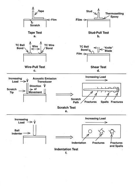
There are literally hundreds of adhesion tests that have been described in the literature [1-5]. Figure 1 shows some of the most common tests.

Figure 1: Some common adhesion tests (fig. 12.3 [1])

The tape (peel) test uses an adhesive tape applied to the film and then peeled from the surface [6]. Usually the coating is scratched before the tape is applied to provide a fracture initiation site(s). This test has many variables (type of tape, angle of peel, rate of pull, etc.) and reveals poor adhesion but does not quantify better adhesion (i.e. it is mostly qualitative). It has the advantage of revealing spots of poor adhesion (“pullouts”) due to contamination such as dust particles. The pullout material is left on the tape.

The pull (tensile) test uses a wire or golf-tee-shaped stud bonded (glued, soldered, ultrasonic bonded) to the coating surface and pulled to failure under tensile stress. This test has the problem that the bonding process may introduce unknown stresses particularly near the edges. A variation of this test is the shear test that uses a blade to push on the side of a bump bonded to the surface. The shear test may also be performed in a lap-shear configuration. The wire bonded pull test maybe used in a non-destructive mode by just pulling to a specified value.

The scratch test is performed by moving a progressively loaded stylus over the surface until fracturing or deadhesion is detected optically [7-9]. The test is very dependent on the stylus shape and material and the physical/mechanical properties of the coating material. The scrape test is a more crude form of the scratch test and might be called a wear (abrasion) test. To further characterize the behavior of a scratch the acoustic emission during scratching may be monitored.

The indentation test uses a progressively loaded indenter and detecting the fracturing and spalling of the coating around the indenter impression. The indentation test is used most frequently for hard coatings. The indentation test is dependent on the physical and mechanical properties of both the coating and the substrate material though the use of microindentation techniques may minimize the effects of the substrate material.

The adhesion of a film or coating to a substrate may increase or decrease with subsequent processing, environments or with time. This change in adhesion may be caused by a number of effects such as diffusion to or away from the interface, stress relief, void formation in the interfacial region, deformation by repeated stressing, chemical effects, etc. Accelerated aging may be used to try to duplicate some or all of these effects but consideration must be given to the fact that interactions between mechanisms may provide misleading adhesion results. For example, heating may increase diffusion rates but may also give stress relief.

Conclusion

 A reproducible adhesion test program can give a useful comparative measure of the practical adhesion* to help ensure that the deposition process is reproducible and the product is adequate for the function and service life of the product. Adhesion measurement values should never be presented as an absolute or “basic” [2,3] property of the system.

* The term practical adhesion is used to include failure in the interfacial region or in “near-by” substrate or coating material [10].

References

  1. D.M. Mattox, “Adhesion and deadhesion,” Ch. 12 in Handbook of Physical Vapor Deposition (PVD) Processing, 2nd edition, Donald M. Mattox, Elsevier (2010)
  2. K.L. Mittal, “Adhesion measurement of films and coatings: a commentary,” pp. 1-15 in Adhesion Measurement of Films and Coatings, K. L. Mittal editor, VPS (1995)
  3. ASTM Proc. of Conf. on Adhesion Measurement of Thin Films, Thick Films and Bulk Coatings (STP 640), edited by K.L. Mittal, ASTM, (1978)
  4. K.L. Mittal, “Adhesion measurement of thin films” Electrocomponent Sci. Technol., 3, 21-42 (1976); References to adhesion testing history and prior review articles
  5. Adhesion Measurement Methods – Theory and Practice, Robert Lacombe, CRC, Taylor and Francis (2006)
  6. ASTM D3359-17 “Standard methods for rating adhesion by tape test”
  7. P.A. Steinmann and H.E. Hinterman, “A review of the mechanical tests for assessment of thin-film adhesion,” J. Vac. Sci. Technol. 7(3) 2267 (1989)
  8. G. Aldrich-Smith, N.M. Jennett and J. Housden, Mechanical Property Measurement of Thin Films and Coatings: A Round Robin to Measure the Adhesion of Thin Coatings, VAMAS TWA 22, NPL Report DEPC-MPE 001 (Sept. 2004)
  9. H.E. Hinterman, “Characterization of surface coatings by the scratch adhesion test and by indentation measurements,” ‘Fresenius’ J. Analytical Chem. 346(1-3) 45-52 (1993)
  10. Donald M. Mattox, “Thin-film adhesion and adhesive failure,” pp. 54-62 in [3]


Adhesion of Vacuum Deposited Films and Coatings. Part 1: Introduction

Part 1: Introduction

Author: Donald M. Mattox

Vacuum deposition may be defined as the deposition of a film and coating by atom-by-atom or molecule-by-molecule on a suitable substrate surface. The vacuum is necessary for the transport of the atom/molecule from the source to the substrate by having a long mean path for collision in the vapor state and for controlling the partial pressure(s) of gaseous reactive species in the deposition environment.

Vacuum deposition may be accomplished by: 1) deposition of vapors from the source material(s) with no reaction on the substrate, 2) reaction of co-deposited materials on the substrate or 3) reaction of the deposited material with the gaseous environment (“reactive deposition”). Vapor sources include: 1) thermal evaporation or sublimation from solid or liquid, 2) sputtering from a solid cooled surface, 3) vaporization from an arc moving over a solid surface, or 4) decomposition of a chemical vapor precursor. In some cases a low pressure plasma may be used to “activate” reactive species and/or provide ions for concurrent energetic particle bombardment of the depositing species (sometimes called “atomic peening”).

The terms “vacuum deposited thin film” and “vacuum deposited coating” are used in the literature without any definition of the thickness or mass per unit area. Early use of vacuum deposition was to deposit films for reflecting and antireflecting films both of which require film thicknesses on the order of a quarter of the wavelength of visible light or about 150 nanometers. This seems to be a logical upper limit for the thickness of a vacuum deposited thin film. At this thickness the physical and mechanical properties of the film often are not important for adhesion. As the vacuum deposit becomes thicker it would be logical to call them thick films but this terminology has a specific meaning in hybrid microelectronics. Therefore the term coating seems to be a good compromise. The properties of the coating may have a significant effect on the adhesion of the coating to the substrate.

Adhesion is the mechanical strength joining two different materials (designated A and B) and is a fundamental requirement of most vacuum deposited films and coatings. In a few cases such as fabrication of free-standing structures, the adhesion may be made deliberately low. The loss of adhesion is sometimes called deadhesion in adhesion technology.

In practical (“apparent”) adhesion the loss of adhesion is by fracture and may be at the actual interface of A&B or may be in A or B (“near interfacial region”) or in an interfacial material A/B that is developed between A and B. This interfacial material is sometimes called the interphase material. The A/B interphase material may be an alloy, a mixture, or a compound of the A&B material or may be a reaction product of the A or B material with the ambient gas/vapor or codeposited material such as an oxide or carbide (see later blog – Types of interfaces)

Fractures are caused by mechanically stressing the interfacial region thus providing energy for fracture propagation. Fractures may be classed, as brittle fracture where there is little plastic deformation and comparatively little energy is needed to propagate a crack in the “brittle” material. If the fracture involves significant plastic deformation to separate the surfaces the failure is called ductile fracture and requires significantly more energy to propagate the failure. In brittle fracture often very little energy must be added to propagate the crack while in ductile fracture more and continuous energy must be supplied to propagate the crack. A material that is both strong and ductile is often called a “tough” material.

Corrosion may enable fracturing by embrittling the material at a crack tip such as is the case with moisture at the crack tip in glass, (a glass-cutter will scribe the glass, then wet the scratch, before applying the stress needed to break the glass) [1] or by “wedging” of the crack by corrosion products.

Fractures may be “blunted” by having the propagating fracture encounter a “tougher” material or by having to change the direction of propagation because of a change in the stress vector.

In vacuum coating, generally fractures are caused by mechanical stresses applied to the interfacial region. If the stress is normal (perpendicular) to the plane of the interface it is call a pure tensile stress. If the stress is parallel to the plane of the interface the stress is call pure shear stress. Of course the applied stress usually will have both a tensile and a shear component due to the direction of the applied stress and/or the roughness of the interfacial region.

The stress that appears at the interface is composed of intrinsic stress and extrinsic stress. The intrinsic stress is the “grown-in” (growth) stress due to the deposition conditions and may vary through the thickness of the deposit. The extrinsic stress is due to external factors such as differences in the coefficient of expansion of the substrate and coating material. The total value of these stresses depends on the thicknesses of the stressed regions. Very thin films may have high stress but still be adherent whereas thick deposits may have such a high total stress that there will be spontaneous deadhesion. For example chromium is often used as a “glue” layer for metallization on glass. Vacuum deposition by thermal evaporation will give a high tensile stress and up to several tens of nanometer thickness will exhibit good adhesion while hundreds of nanometers will cause fracturing in the near-surface region of the glass.

Fractures in brittle materials often have point of fracture initiation where there is a defect or where stresses are concentrated. Microcracks or scratches in the surface of a brittle material, such as glass, are an example of fracture initiation sites.

Deadhesion may be local, creating “pull-outs” or “pinholes.” Common sources of pinholes are dust particles and “spits” or “macros” from arc vapor deposition. The pinholes may act as initiation sites for further fracturing.

Other types of time-dependent stresses such as interfacial corrosion may cause deadhesion. Deadhesion by weakening of the adhesion bonding may also result from diffusion to or from the interfacial region by chemical species or structural defects such as voids. In some cases diffusion may result in strengthening of the adhesive bond.

Designing for adhesion in vacuum deposition requires an understanding of the substrate and coating materials involved, their interaction, and how the deposition process influences their properties. This in turn requires an understanding of the condensation and nucleation of the depositing material, the interface formation and the nature of the film growth. Even monolayers of contamination may influence nucleation and growth so control of contamination prior to and during vacuum deposition is important in having a reproducible vacuum deposition process.

Reference

  1. M. Tomozawa, “Fracture of glasses,” Annual. Rev. Mat. Sci. 26, 43-74 (1996)


Ion Plating: a personal account of the early years

Author: Donald M. Mattox

It all began with vacuum cadmium plating of high strength steel compressed gas bottles.

After serving as a meteorologist and Air Weather Officer in the USAF during and after the Korean War, I obtained a M.S. degree in solid state physics from the University of Kentucky in 1961 (see more in Endnote A).

I reported to Sandia Corporation in April of 1961 as a Technical Staff Member and began work as a solid-state physicist in the metallurgical engineering group. The Sandia “metallurgy group” was composed of a mix of material science people with specialties ranging from metallurgy, organic adhesives, surface cleaning, and ceramic fabrication, to process “troubleshooters” and technology transfer. In order to learn more about material science I began teaching a noon-hour course on material science for interested laboratory personnel – I was teaching the course when President John F. Kennedy was assassinated on Nov. 22, 1963.

The metallurgy department had an old CVC vacuum system that wasn’t being used. It had a glass bell jar with a cable hoist, a manually cranked high vacuum gate valve, and an oil diffusion pump. I had done some vacuum work at University of Kentucky so I decided to get it working.

My “bible” was Leslie Holland’s book Vacuum Deposition of Thin Films (1956) (Chapman Hall). I got the system into operation with a filament evaporator then added a DC sputtering capability. I controlled the pressure for sputtering by manually “cracking” the gate valve. My mass flow controller was a manual needle valve. I had a CEC LC-031 DC high voltage power supply that used mercury thyratron rectifier tubes. It could get to 5000 volts DC though it tended to arc internally at the high voltages. When the sputtering cathode arced the voltage would go down, the current would go up, the tubes would light up and the plates in the high voltage transformer would buzz. The only way to turn off a “hard arc” was to manually turn off the power supply – there was no arc suppression/quenching circuit in that power supply!

One of my first troubleshooting trips was to a contractor’s processing line for applying vacuum deposited cadmium (“VacCad”) plating to high-pressure gas bottles. They were having problems with the adhesion of the cadmium coating to the steel. The problem was simple – they were blowing off the part with “house air” and the air contained oil from the compressor. That got me thinking about the adhesion of vacuum deposited coatings [1]. When I discussed this with the metallurgists they maintained that to get good adhesion you needed solid solubility. Being a solid state physicist I thought just getting good atom-to-atom contact should give you good adhesion.

In the library I found that the field of high vacuum surface science studies on atomically clean surfaces really began in the mid-1950s when H. Farnsworth produced atomically clean surfaces by repeated sputtering and annealing in high vacuum [2,3]. I thought “What if you started depositing using thermal evaporation while you are sputtering the substrate surface. Might that not give a “clean” interface and good atom-to-atom contact?” So in one afternoon I tried vacuum evaporation while the sputter cleaning was still going on. It worked great! When I evaporated copper into the plasma there was a nice green glow indicating excitation/de-excitation of the copper atoms and probably ionization.

I decided that the definitive experiments should involve immiscible materials so I chose silver and iron, which are immiscible even in the molten state. I coated a series of iron tensile bars with silver and elongated them to test the adhesion. My “ion plating” technique gave adhesion greater than that detectable by the test.

I presented the work at a Gordon Research Conference on Adhesion in the summer of 1963. My paper (“Deposition by Exploding Wire and Ion Plating”) was scheduled for presentation on Thursday evening. On Wednesday I had yet to received permission to present the paper because a patent application was being made. On Thursday I received permission to present the paper. After the Thursday evening all-you-can-eat lobster dinner I was completely full of lobster and gave the paper. The paper and the subsequent discussion went on for 3 hours! The concept of ion plating was first published in the technical literature in 1964 [4] and the patent was issued in 1967 [5]. Of course in hindsight, there was very little ionization of the evaporated material in the plasma that I used – bombardment was mainly by the inert gas ions used for sputtering.

The 1967 (priority 1964) ion plating patent covered the use of both thermal evaporation and chemical vapor precursors as sources for the depositing material [6]. In 1969 (priority 1964) H.F. Sterling and R.C.G. Swann patented the use of chemical vapor precursors in an RF plasma with no substrate bias as a means of depositing coatings by what was later called plasma enhanced chemical vapor deposition (PECVD) [7,8].

Bob Culbertson of EIMAC/Varian expressed an interest in using the ion plating process for metallized ceramics at a low temperature and we metallized ceramics using a WCl4 precursor [9]. Bob later patented ion plating for depositing low-electron-emission coatings (C and TiC) on electron tube grids [10]. One of the claims in his 1971 patent (filed 1968) used both a filament evaporator and a chemical vapor precursor to deposit coatings such as TiC. This was the first use of ion plating as a hybrid deposition process of PVD/PECVD. His patent was probably the first report on what came to be known as “reactive ion plating” [11]. Y. Murayama was the first to use the term “Reactive Ion Plating” in the peer-reviewed literature in 1975 [12]. The Japanese seemed to pick up the use of the term “ion plating” much more quickly than did others.

The term “ion plating” was used in the 1967 paper published in Electrochemical Technology and in the patent. The term came under some criticism and was discussed in the Journal of the Electrochemical Society in 1968 [13]. Over the years others have used different terminology for much the same process. These include: Ion Vapor Deposition (IVD), Ionized Physical Vapor Deposition (iPVD), Ion Assisted Deposition (IAD), Ion Beam Assisted Deposition (IBAD), Biased Activated Reactive Deposition (BARE), and Energetic Condensation.

The Sandia reactor group was developing nuclear reactors for providing pulses of neutrons; the SPR series of pulsed neutron reactors [14]. The SPR II reactor contained 105 kg of U-Mo alloy of which 93% of the uranium was 235U (more than the 64 kg that was in the gun-type “Little Boy” atomic bomb of WW II). When pulsed by bringing the components together, the uranium parts attained very high temperatures very quickly. In the SPR I reactor the uranium was protected by electroplated nickel and the nickel had to be periodically replaced. The old nickel had to be chemically stripped and the surface “pickled” all of which was undesirable since they lost some 235U in the process and the surface was roughened. They wanted a substitute for the electroplated nickel coating.

We ion plated samples of depleted uranium with aluminum and subjected them to corrosion tests, which it passed with flying colors [15]. We then coated some mock-ups of the reactor components. When it came to coating the real parts we had to strip the nickel and then pump down overnight – all the while with an armed guard by our side. The coated parts worked very well [16].

In analyzing the coating substrate-coating interface we found that there was an appreciable layer of UAl2 formed at the interface due to the clean interface, the heating from the sputter cleaning, and thermal diffusion during the deposition.

While we were working on the uranium project we were also developing other fixtures for ion plating, several of which were described in the patent. These included a “cold finger” fixture for keeping the back-side of the sample cooled to liquid nitrogen temperature during deposition. We used that technique to deposit metallization electrodes on semiconductor materials to avoid “pipe diffusion”.

We were also using a rotating cage fixture (patterned after the barrel plating technique used in electroplating) for coating small parts [17]. Ion plating using the cage fixture was used to vacuum coat ultra-high vacuum components with gold to reduce hydrogen outgassing.

The ion plating patent also covered the use of a grid in front of an insulator or irregular surface to provide bombardment. We used this arrangement to coat ceramics and polymers [18,19]. Ion plating was also used to coat metals with chromium for glass-to-metal sealing [20].

The use of ion plating for aluminum coating spread quickly through the AEC nuclear weapons complex for coating uranium and plutonium as well as silver on beryllium for diffusion bonding [21]. R.T. Bell and J.C. Thompson at the Oak Ridge Y-12 Plant used ion plating as a “strike” for electroplating in 1973 [22] as did others [23].

In January 1965 Time Magazine ran a short news item called “Plating with a permanence” about the ion plating process and the article caught the attention of McDonnell-Douglas. They sent a group to look at what we were doing. They saw the rotating cage fixture and they took the idea back and developed their “IVADIZING” machine for coating fasteners for the aerospace industry [24-26]. This became the basis for the IVD (“ion vapor deposition”) process, which is widely specified for military and aerospace applications [27].

T. Spalvins and Donald Buckley of NASA (Cleveland) picked up the ion plating process for their studies of lubrication in space using low-shear metal films [28]. Based on the NASA work General Electric began using ion plating for coating their X-ray tube bearings with low shear metals for lubrication in vacuum. The dissemination of the ion plating process was aided by the fact that the patent was in the public domain.

In the sixties, RF sputtering began to be used for sputtering dielectric materials. I converted an old diathermy machine for RF sputtering. We began to sputter dielectric materials [29]. Several months after we began rf sputtering FCC inspectors showed up! We had been broadcasting all over the radio spectrum and my laboratory was right by the runway at Kirkland AFB. We were interfering with the aircraft-to-ground communication. Since we were only doing it sporadically they had a hard time finding us. I was shut down – but the “powers that be” at Sandia then purchased an RF system for my group with proper shielding.

The mid-sixties was also the time that scanning electron microscopy (SEM) was coming onto the scene as a commercially available analytical tool [30] (1965 – Cambridge Scientific Instruments – “Stereoscan”). I began to look at the fracture cross-section morphology of thick ion plated coatings. It was immediately obvious that ion bombardment during deposition was disrupting the columnar growth and densifying the deposit as well as affecting the surface morphology [31,32]. For a period of time the densification by bombardment was called “atomic peening” [33] though this descriptive terminology has fallen out of favor.

At about the same time as I was doing the ion plating work using thermal evaporation, several others were doing similar work using “bias sputtering” [34-37]. However, they did not seem to do much analytical work on the films other than that related to the function they were studying. Some authors later called this process “sputter ion plating [38].

In the early work on ion plating it was found that ultrafine particles were deposited on the interior walls of the chamber but not on the negatively biased substrate [39]. The particles that formed in the plasma attained a negative charge and were repelled by the negative potential on the substrate. Later the same phenomenon was observed in high rate sputtering [40,41].

In the case of reactive materials such as titanium, the deposited ultrafine particles were stable when exposed to air, apparently because of a very thin surface oxide layer. When disturbed the fine particles would “burn.” To quote from Handbook of Physical Vapor Deposition Processing, 2nd edition (2010) (p. 322, section 9.9.2), Donald M. Mattox, Elsevier.

“In the early work on ion plating, the particles formed in the plasma and deposited on the walls were called ‘black sooty crap’ (BSC) and could be very combustible. One game was to ask an observer to wipe the particles off a window with a paper towel. When the window was wiped, the towel caught fire and a flame front moved over the interior surface of the chamber, which was covered with BSC.”

In hindsight I wish that I had done more studies on the charged ultrafine particles since 20 years later ultrafine (nano-) particles became an important field of study.

By the mid 1970s several papers had been published on how ion plating could be used to tailor the properties of thick deposits using both continuous and periodic bombardment during deposition. It was well established that forming the interface by beginning the deposition during sputtering cleaning gave good adhesion, bombardment with reactive ions allowed reactive deposition of dense compound materials, and bombardment during deposition could be used to control intrinsic stress, morphology, and crystallographic orientation of the deposited coating materials.

In the book chapter “Ion Plating Technology” in the first edition of Deposition Technologies for Films and Coatings, Development and Applications edited by R.F. Bunshah et al (1982) a rather extensive bibliography of papers on ion plating and related subjects was provided for the period 1963 to 1980 [42].

With the advent of arc vaporization in the early 1980s [43], and HIPIMS in the early 2000s [44] where a large percentage of the vaporized material is ionized to condensable “self-ions,” bombardment effects on the properties of coatings entered a new realm [45].

Some time in the early 1970s someone called attention to the fact that Bernard Berghaus, of plasma nitriding fame, had patented a process similar to “ion plating” in Europe in the mid-1930s [46]. His work in this area seems to have been an extension of his earlier work on ion nitriding and sputter deposition [47-49]. Berghaus apparently did not pursue any application of the process nor did he publish anything in the technical literature about the process that I could find. Leslie Holland didn’t discuss Berghaus’ coating work in his book Vacuum Deposition of Thin Films so it must not have been well known at that time (1956).

By the mid-70s my group became involved in solar energy (depositing selective solar thermal absorbers), fusion reactor technology (coating TOKAMAK limiters) and in developing a lithium source for the Sandia fusion PBFA fusion reactor experiments. Ion plating just became another “tool.”

Using ion plating for tailoring the coating stress was carried over into stress control for the deposition of thick Mo coatings for the BOLVAPS lithium ion source for Sandia fusion energy experiments. At low pressure sputtering the high energy reflected neutrals from the sputtering target may bombard the deposit and affect the stress in the deposit [50]. The technique of “pressure pulsing” for stress control in the sputter deposition of thick deposits was developed to tailor the stress in thick sputter deposited coatings [51]. Pressure pulsing relies on bombardment by high-energy reflected neutrals from the sputtering target at a low pressure environment rather than accelerating ions from a plasma.

In a 2013 publication Professor Allan Mathews, University of Sheffield, Sheffield, UK, credited Ion Plating with being the “First Wave” of “Plasma Assisted PVD Processing” [45].

Conclusion:

The quest for better adhesion by having a clean interface led to a serendipitous way to modify film/coating properties (optical, metallurgical, electrical, chemical, etc.) by energetic particle bombardment during deposition of PVD and PECVD films/coatings.

Acknowledgements:

From the mid-1960s and through the following years I had a number of technicians and several staff members who worked with me on ion plating projects. Notable among the technicians were: Frank Rebarchik, Ray Bland (who later became a Laboratory {shop} Supervisor), George Kominiak (who later became a Technical Staff Member), and Chuck Peeples. Notable among the technical staff members were: Bob Cuthrell, Ray Berg, Janda Panitz, Don Sharp, Art Mullendore, Jack Houston, and John Whitley. Special thanks to my supervisors who gave me the leeway to pursue ion plating projects. These include, in the early years: John McDonald, Charlie Bild, Lou Berry, Bill O’Neal and Dick Schwoebel. Thanks also to Lew Jones who took me under his wing when I first arrived at Sandia and taught me some of the nuances of troubleshooting at production facilities.

Endnote A: I graduated from Eastern Kentucky State University during the Korean War. I joined the USAF for four years to become an officer and be trained as a meteorologist. I attended two semesters of meteorology at Massachusetts Institute of Technology (MIT) (1953-54) before being deployed to Eglin AFB, FL as a weather forecaster.

After a year I was assigned to the 58th Weather Recon Sq. at Eielson AFB, Alaska as an Air Weather Officer. My job was as an in-flight weather observer on synoptic weather fights that also included air sampling for detecting Russian nuclear tests. The flight routes were over the Bering Sea to Attu at the western end of the Aleutian Island chain and north to near the North Pole. I flew about 1500 hours in B-29 and then B-50 aircraft.

After leaving the USAF I went to graduate school at the University of Kentucky (Lexington, KY) under the GI Bill. I was in the Physics Department and was a graduate assistant in the Solid State Physics laboratory. My advisor was Professor Lee Gildart. In 1960 Dr. Gildart left unexpectedly and I was offered a position in the High Energy Physics lab counting cloud chamber tracks. No way was I interested in doing that! That sent me looking for a job.

I wanted to move to the Southwest so I traveled around CO, AZ, NM interviewing. I had noted that Sandia Corporation, a US Atomic Energy Commission (AEC) laboratory run by AT&T in Albuquerque, NM used bicycles to get around their Technical Area but I didn’t know much about what they did (about 6 months after I went to work for Sandia they quit using bicycles in the Tech Area). At their Personnel Office I said that I wanted to interview for a staff member position. It turned out that this was pretty unusual in that Sandia usually went to universities to recruit and had very few “walk-ins” for a technical staff member position.

Personnel had several people from the Metallurgy Group come over for an interview. Up to that time the metallurgy group had been “handbook engineers” but they wanted to expand into R&D. They asked “Can you do research?” Of course I said yes since I had co-authored several peer- reviewed papers while at the U of K. They offered me $750 per month salary – a magnificent sum compared to what I was making at U of K!

I had the option of going to work immediately outside the technical (“tech”) area in the “leper colony” and wait for my security clearance or return in about 6 months after I had a clearance. I chose to wait since I wanted to finish my Masters Degree [A-1]. This was the beginning of my work and sojourn at the Sandia National Laboratories until I retired in 1989 to become active as a consultant and course instructor in Management Plus, Inc. (MPI) with my wife Vivienne. MPI is a consulting and education training organization in the field of vacuum coating.

A-1. D.M. Mattox and L. Gildart, “Energy gaps in bismuth trioxide,” J. Phys. Chem. Solids 18(2-3) 215 (1961)

References:

  1. D.M. Mattox and J.E. McDonald, “Interface formation during thin film deposition,” J. Appl. Physics 34, 2493 (1963)
  2. H.E. Farnsworth, R.E. Schlier, T.H. George and R.M. Burger, “Ion bombardment cleaning of germanium and titanium as determined by low-energy electron diffraction,” J. Appl. Phys, 26, 252 (1955)
  3. H.E. Farnsworth, “Preparation, structural characterization, and properties of atomically clean surfaces,” (AVS Welch Award presentation) J. Vac. Sci. Technol., 20, 271 (1982): doi: 10.1116/1.571282
  4. D.M. Mattox, ”Film deposition using accelerated ions,” Electrochem. Technol. 2, 295 (1964); Sandia Corp. Development Report SC-DR-281-63 (1963)
  5. Donald M. Mattox, “Apparatus for coating a cathodically biased substrate from plasma of ionized coating material,” USP 3329601 (priority date, Sept. 5, 1964; filed, Sept. 30, 1966; publication, July 4, 1967) (assigned USAEC)
  6. D.M. Mattox, “Tungsten CVD in a gas discharge,” Sandia Corp. Development report, SC-DC-67-2026A (1967); presented at the “Conf. on Chemical Vapor Deposition of refractory metals, alloys, and compounds,” Gatlinburg, TN (Sept. 12-14, 1967)
  7. Henry Frank Sterling and Richard Charles George Swann, “Method of forming silicon nitride coating,” USP 3485666 (priority date, 8 May 1964; filed, 3 May 1965; published, 23 Dec. 1969) (assigned International Standard Electric Corp.); British pat. 1104935; French pat. 1442502
  8. R.C.G. Swann: https://ethw.org/w/index.php?title=Special:Search&search=The+Birth+of+Glow+Discharge+Chemistry+%28aka+PECVD%29+-+extensive+references&searchToken=chbbl6060oeonkahx2lto80hu – extensive references
  9. R. Culbertson and D.M. Mattox, “High strength ceramic-metal seals metallized at room temperature,” 8th Conf. Tube Technol. IEEE Conf. Record TK 6563, 3, U52, p. 101 (1966)
  10. Robert D. Culbertson, Russell C. McRae, and Harold P. Meyn, “Nonemissive electrode structure utilizing ion-plated nonemissive coatings,” USP 3604970 (filed 14 Oct. 1968; published 14 Sept. 1971) (assigned Varian Assoc.)
  11. Donald M. Mattox, “Short history of reactive evaporation,” pp. 50-51, SVC Bulletin, Society of Vacuum Coaters (Spring 2014)
  12. Y. Murayama, “Thin film formation of InO2, TiN and TaN by RF reactive ion plating,” J. Vac. Sci. Technol. 12, 818 (1975)
  13. Discussion on “Adherence and porosity of ion plated gold,” C.F. Schroeder and J.E. McDonald, J. Electrochem. Soc., 115(12) 1255 (1968) – Reply by Donald M. Mattox
  14. T.R. Schmidt and J.A. Reuscher, “Overview of Sandia National Laboratories pulse nuclear reactors”, SAND-94-2466C (1994); also CONF-941102-28 (Conference: Winter meeting of the American Nuclear Society (ANS), Washington, DC, 13-18 Nov 1994); OSTI ID: 10190030
  15. R.D. Bland, J.E. McDonald, and D.M. Mattox, “Ion plated coatings for the corrosion protection of uranium,” Sandia Development Report SC-DR-65-519 (1965)
  16. D.M. Mattox and R.D. Bland, “Aluminum coating of uranium reactor parts for corrosion protection,” J. Nucl. Mater., 21, 349 (1967)
  17. D.M. Mattox and F.N. Rebarchik, “Sputter cleaning and plating small parts,” Electrochem. Technol., 6, 74 (1968)
  18. D.M. Mattox, “Metallizing ceramics in a gas discharge,” J. Am. Ceramic Soc. 48, 385 (1965)
  19. “High strength ceramic-metal seals metallized at room temperature,” R. Culbertson and D.M. Mattox, 8th Conf. Tube Technol., IEEE Conf. Record TK 6563, 3, U52, p. 101 (1966)
  20. D. M. Mattox, “Chromizing molybdenum for glass sealing,” Rev. Sci. Instrum. 37, 1609 (1966)
  21. G. Mah, P.S. Mcleod, and D.G. Williams, “Characterization of silver coatings deposited from a hollow cathode source,” J. Vac. Sci. Technol., 14, 152 (1977)
  22. R.T. Bell and J.C. Thompson, “Applications of ion plating in metals fabrication,” Oak Ridge Y-12 Plant, Y-DA-5011 (1973)
  23. J.W. Dini, “Ion plating can improve coating adhesion,” Metal Finishing, 91(9) 15-20 (Sept. 1993)
  24. K.E. Steube and L.E. McCrary, “Thick ion vapor deposited aluminum coatings for irregular shaped aircraft and spacecraft parts,” J. Vac. Sci. Technol., 11, 362 (1974)
  25.  J. Carpenter, G. Kesler, A. Klein, L. McCrary, and K. Steube, USP “Glow discharge coating apparatus,” 3750623 (filed 11 Feb 1972; published 7 Aug. 1973) (assigned to McDonnell Douglas Corp.)
  26. Kenneth E. Steube, “Glow discharge-tumbling vapor deposition apparatus,” USP 2926147 (filed 15 Nov 1974; published 16 Dec. 1975) (assigned to McDonnell Douglas Corp.)
  27. MIL-DTL-83488D; “Coating; High purity aluminum,” (01 April 1999); superseding MIL-C-83488C, “Coating; Aluminum ion vapor deposited,” (01 Dec. 1978)
  28. T. Spalvins, J.S. Przbyszewski, and D.H. Buckley, ”Deposition of thin films by ion plating on surfaces having various configurations,” NASA Lewis TN-D3707 (1966)
  29. G.J. Kominiak and D.M. Mattox, ”Physical properties of thick sputter deposited glass films,” J. Electrochem. Soc. 120, 1535 (1973)
  30. C.W. Oatley, W.C. Nixon and R.F.W Pease, “Scanning electron microscopy,” Adv. Electron Phys., 21, 181 (1965)
  31. D.M. Mattox and G.J. Kominiak, ”Structure modification by ion bombardment during deposition,” J. Vac. Sci. Technol. 9, 528 (1972)
  32. R.D. Bland, G.J. Kominiak, and D.M. Mattox, ”Effects of ion bombardment during deposition on thick metal and ceramic deposits,” J. Vac. Sci. Technol., 11, 671 (1974)
  33. A.G. Blackman, Metall. Trans. 2, 699 (1971)
  34. G.K. Wehner, ”Growth of solid layers on substrates which are kept under ion bombardment before and during deposition,” USP 3,021,271 (filed April 27, 1959, publication, Feb, 1962)
  35. R. Frerichs,”Superconductive films by protected sputtering of tantalum or niobium,” J. Appl. Phys., 33, 1898 (1962)
  36. L.I. Maissel and P.M.Schaible, “Thin films formed by bias sputtering,” J. Appl. Phys., 36, 237 (1965)
  37. Orla Christensen, “Characteristics and applications of bias sputtering,” Solid State Technology, p. 39 (Dec. 1970)
  38. N.M. Renevier, V.C. Fox, D.G. Teer, and J. Hampshire, “Coating characteristics and tribological properties of sputter-deposited MoS2/metal composite coatings deposited by closed-field unbalanced magnetron sputter ion plating,” Surf. Coat. Technol., 127(1) 24 (2000)
  39. “A short history of ultrafine (nano-) particles formed in vacuum,” Donald M. Mattox. pp. 54-56, SVC Bulletin, Society of Vacuum Coaters (Summer 2014)
  40. G. Selwyn, J. McKillop, K. Haller and J. Wu, J. Vac. Sci. Technol., A8, 1726 (1990)
  41. G. Jellum and D. Graves J. Appl Phys., 67, 6490 (1990)
  42. “Ion Plating Technology,” Donald M. Mattox, Ch. 6, pp. 244 – 268, in Deposition Technologies for Films and Coatings: Development and Applications, edited by R. F. Bunshah et al, Noyes Publications (1982)
  43. I.I. Aksenov, V.A. Belous, and V.E. Strel’nitskij, “Vacuum-arc surface modification and coating deposition methods in KIPT, Ukraine (Historical Review)” Proceedings 55th Annual Technical Conference, pp. 3-8 Society of Vacuum Coaters (2012); also pp. 48-52, SVC Bulletin, Society of Vacuum Coaters (Summer 2012)
  44. A.P. Ehiasarian, R. New, W-D. Munz, L. Hultman, U. Helmersson, V. Kouznetsov, “Influence of high power densities on the composition of pulsed magnetron plasmas,” Vacuum 65 (2) 147–154 (2002) doi:10.1016/S0042-207X(01)00475-4
  45. Allan Matthews, “Plasma Assisted PVD: The Past and Present,” p. 24-27, SVC Bulletin, Society of Vacuum Coaters, (Fall 2013); also Keynote paper ISSP 2013 (12th International Symposium on Sputtering and Plasma Processes) July, 2013, Kyoto, Japan
  46. “Improvements in and Relating to the Coating of Articles by Means of Thermally Evaporated Materials,” B. Berghaus, UK Patent# 510, 993 (priority date Aug. 26, 1937, filed Aug. 23, 1938, issued Aug.11, 1939)
  47. B. Berghaus, “Improvements in and relating to the coating of articles by means of thermally vaporized material,” UK patent #510,993 (filed; publication 1938); also “An improved process for metallizing metallic articles by means of cathode disintegration in vacuum,” UK patent #520592-A (priority date, Nov. 19, 1937, publication date, Oct. 26, 1938).
  48. Wilhelm Burkhardt and Rudolf Reinecke, “Method of Coating Articles by Vaporized Coating Material,” USP# 2,157,478 (priority date, June 17; 1936; filing date, June 15; 1937, publication May 9, 1939) (assigned to Bernard Berghaus) – thermal evaporation source
  49. Wehnelt Eilhart, Hermann Ramert, Wilhelm Burkhart, “Coating of articles by means of cathode disintegration,” USP 2,239,642 (priority date , May 27, 1936; filing date, May 21, 1937; publication date, April 22, 194) (assigned to Bernard Berghaus) – sputtering source
  50. J.A. Thornton and D.W. Hoffman, “Internal stresses in titanium, nickel, molybdenum and tantalum films deposited by cylindrical magnetron sputtering,” J. Vac. Sci. Technol. 14, 165 (1977)
  51. D.M. Mattox, R.E. Cuthrell, C.R. Peeples and P.L. Dreike, “Preparation of thick stress-free Mo films for a resistively heated ion source,” Surf. Coat. Technol., 36, 117-124, 1988


Safety Aspects of Cleaning

Author: Donald M. Mattox

Many materials used for cleaning have hazardous properties such as the ability to irritate or chemically “burn” skin; be toxic, carcinogenic, or mutagenic, cause degeneration of body organs, such as the liver (many solvents), or lungs (acids, chlorine, ozone); or be flammable or explosive. The Material Safety Data Sheets (MSDSs) for hazardous materials (HazMats) should be readily available because they contain information about the hazards, recommendations for use and storage, and first-aid procedures (where applicable). USA law requires that MSDSs for all chemicals used in the workplace be made available to the workers using those materials.

Gases and vapors are often the most hazardous form of materials encountered in the workplace. The hazards may be due to flammability or they may be toxic if inhaled. Generally there is a level, given in parts per million by volume (ppmbv) or weight per volume (mg/m3), below which, the material is not considered hazardous.

The Threshold Limit Value (TLV) or Permissible Exposure Limit (PEL) is the concentration of gas or vapor to which an average worker can be exposed on a continuous eight-hour-shift basis, day after day, without suffering ill effects. For example, for isopropyl alcohol the TLV is 400 ppmbv or 980 mg/m3, while for ozone (O3) it is 0.1 ppmbv. Because of the difference in susceptibility of different people to different chemicals, it should be recognized that there should be exceptions to these limits. These values are continually changing so reference should be made to the latest values from OSHA (www.osha.gov).

Frequent exposure is measured as a Time-Weighted Average (TWA) value over the term of the exposure. The exposure can exceed the TLV value for some period of time but still keep the average value within the TLV limits. The maximum exposure, under these circumstances is given by the Short-Term Exposure Limits (STEL). For example, the STEL for trichloroethylene (TCE) is 200 ppmbv while the TLV is 50 ppmbv.

In some cases there is a ceiling value (“C” limit) or IDLH (Immediately Dangerous to Life or Health) limit to exposure that should not be exceeded at any time. If this value is exceeded, the area should be evacuated immediately. For example, hydrochloric acid (HCl) has a C-value of 5 ppmbv. There are detectors available for measuring the concentration of hazardous gases and vapors and usually they have an adjustable alarm level.

Fires are classified as: Class A—ordinary solid combustible material, Class B—combustible fluids such as petroleum product, Class C—involve energized electrical equipment, and Class D—involve combustible and reactive metals such as magnesium. Fire extinguishers appropriate for the class of the fire to be expected should be available. Some materials, such as vinyl, produce toxic vapors when they burn. More people are killed by inhalation of smoke and vapors than are killed by burns. Great care should be exercised in fighting a fire. Each work area should have a list of the chemicals in the area posted on the door. This alerts firefighters to the possibility of toxic fumes or explosive hazards in the area if there is a fire.

Flammable liquids, such as alcohol, should be stored in appropriate fireproof containers in limited amounts. Materials not being used should be stored away from the use area in fireproof cabinets that prevent overheating of the containers in the event of a fire. Oxidizing and reducing chemical should not be stored in the same cabinet. Chemical containers should be compatible with the chemical they contain and should be clearly labeled as to their content. Flammable liquids can fuel fires and make extinguishing a fire difficult.

The flash point is the temperature at which a liquid or solid will give off enough vapor to form an ignitable mixture with air just above the surface. For example, pure isopropyl alcohol (C3H8O) has a flash point of 12°C, which makes it a very flammable material. The flammable limits give the percent by volume of the material that supports a flame in air. Above or below those limits a flame will not burn by itself. For pure isopropyl alcohol, the flammable limits are 2.3 to 12.7%, while for hydrogen it is 4 to 75%. Acid cleaning can cause the evolution of hydrogen, and acid cleaning should be done in a well-ventilated area with no ignition (spark) source present.

Often the plant Fire Marshal will set the limits on the type and amount of a material that can be used based on the flash point of the material. As a general rule, use of large amounts of materials with a flash point of 140°F in an open area would be banned, while the use of large amounts of materials with a flash point of 165°F or higher is all right. The ignition temperature is the temperature at which there will be self-sustained combustion independent of an ignition source. The ignition temperature of a flammable mixture of isopropyl alcohol is 399°C. Use of low-flash-point materials requires the use of good area ventilation or some type of vapor containment.

Areas where chemicals are used can vary from poorly ventilated open areas to ventilated “chemical hoods,” to fully enclosed processing volumes. Ventilation of an open area is often the first thing to be considered. For example, trichloroethylene (TCE) is a solvent that is nonflammable but is toxic if inhaled. OSHA health standards allow 50 ppmbv of TCE in the air. This standard can generally be met by appropriate area ventilation.

More controlled ventilation can be obtained in a chemical hood that is enclosed except for an opening (face) through which operations are performed in the enclosed work area. Generally this opening may be closed by a sliding window. Air is swept from the outside area, through the face opening, into the work area and out the exhaust. Ventilation is measured by the “face velocity” of the air. A minimum velocity of 100 fpm (feet per minute) is generally used, with higher face velocities used for more toxic materials. In some applications the chemical hood should be fireproof and explosion proof. The exhaust-duct system should be engineered, located, and verified so that the exhaust gases and vapors do not re-enter the building through another ventilation system or pose a threat to people working near the exhaust outlet. Exhaust vents should be clearly marked at the outside location.

The best ventilation control can be obtained in a completely enclosed processing chamber(s). This may be a batch-type system where the parts are placed in a chamber, the chamber is sealed before processing begins, and the chamber is evacuated before the chamber is opened to the ambient. The processing chambers can also be arranged in an air-to-air in-line configuration where parts enter the enclosed processing volume through an entrance chamber and exit through another chamber in a periodic or continuous manner. The inlet and exit chambers may be periodically evacuated or continuously ventilated. A gas “curtain” can also be used to prevent escape or mixing of gases and vapors.

Ozone (O3) is used for cleaning (UV/O3 cleaning) and for water purification. Ozone may be generated by short-wavelength ultraviolet radiation (UVC preferably) or by an oxygen-arc or gas-discharge plasma. Exposure to short-wavelength ultraviolet radiation can be harmful to eyes and promote skin cancer. You can smell ozone (it is what you smell after a lightning storm), but above about 10 ppmbv ozone will kill the olfactory nerves and you will cease to smell it. At concentrations above 10 ppmbv, ozone becomes toxic. As long as you can smell the ozone it is safe for short-term exposure. Ozone should be used in a well-ventilated area and when using UV/O3 cleaning cabinets the ultraviolet light should be turned off when ever the operator opens the door of the cabinet. If you must look at short-wavelength ultraviolet radiation you should be well covered with clothing and wear UV-adsorbing safety glasses (a UV 400 rating provides 100% protection from UVA and UVB radiation but not UVC a).

UVA – 320-400 nm – may be generated with LEDs

UVB – 290-320 nm

UVC – 200-290 nm from mercury vapor glow discharges, quartz envelopes, band pass filtered

EUV – <200 nm – Extreme or vacuum UV

a Do not just use regular sunglasses – the dark glasses cause the iris of the eye to open wide and if the sunglasses are not UV absorbing this increases the harm done by the UV exposure.

Concentrated acids should be added slowly to water because heat is generated during the dilution. The heating can cause splashing so face shields, goggles, and appropriate clothing and gloves should be worn. Never add water to concentrated acid. Generally one of the main first-aid procedures for any chemical accident is flushing with copious amounts of water. The work area should have an emergency shower facility, an eyewash stand, and/or other sources of water available. Eye rinse cups and solutions should be available.

Personnel in the processing area should be trained in basic first aid. This includes cardiopulmonary resuscitation (CPR), stopping blood loss by local pressure, treatment for shock, and first aid relating to specific hazards. It is particularly important that personnel be familiar with in-house and external emergency communication, alarms, and procedures.

Hydrofluoric acid is used for etching and cleaning oxide materials and is a particularly egregious material for causing chemical burns. These burns are progressive unless the residual acid is removed or neutralized. First-aid procedure is to immediately remove contaminated clothing, rinse the area with copious amounts of water, and apply a chemical neutralizing agent. Medical assistance should be obtained immediately. The burn area should be soaked in an iced aqueous or alcoholic solution of benzalkonium chloride (USP 0.1 to 0.133%) for 1 to 4 hours. Soaking may be accomplished using an immersion bath or by a wet compress. Hydrofluoric acid should not be used without appropriate first-aid chemicals available and personnel trained in their use.

Proper clothing for the workplace is important to safety. Eyes and face should be protected from liquids and flying objects by safety glasses, safety goggles, and/or face shields where appropriate. Goggles, and to a lesser extent safety glasses and face shields, also prevent a person from inadvertently rubbing their eyes with contaminated fingers or gloves. Street clothing should be covered by a lightweight coat (smock) that contains loose clothing, such as neckties, and prevents chemical spills from reaching adsorbent materials such as cotton or silk. The smock can be made of an impermeable material such as Tyvek™, a closely woven fabric such as Nylon™, or a breathable material such as GoreTex™. Cotton is not recommended because it is very adsorbing. When using acids, rubber-coated fabric may be used for smocks or aprons.

When handling chemicals, hands can be protected by gloves— polyethylene or vinyl gloves being the most commonly used. When handling acids, rubber gloves are appropriate. When handling hot surfaces, Nomex™ polyamide gloves are a substitute for the asbestos gloves widely used in the past. Nylon™ and Dacron™ are not good materials to wear in a hot environment because they can melt, adhere to the skin, and cause very severe burns. Shoes should be such that chemicals and liquids are not trapped in the shoes if they are spilled. This may mean using high-topped shoes or shoe covers with top closures.

Removal of some types of film deposits from PVD deposition chambers and fixtures can present safety hazards. In particular, heavy metals such as lead, or particles of beryllium, tellurium or selenium can pose a health hazard if ingested. It is best to remove these materials by wet techniques to avoid dust. Refer to Sax’s book for specific safety hazards associated with materials. Often grit blasting is used to strip film buildup from surfaces. If silica sand is used the workers should avoid breathing the dust because it can cause silicosis, a lung disease. Silica sand should be washed and used in a well-ventilated area with workers protected by appropriate respiratory equipment. This potential health hazard can be avoided by using cast-iron grit or alumina grit instead of silica grit.

General References:

  1. Sax’s Dangerous Properties of Industrial Materials, 10th edition, Richard J. Lewis, and N. Irving, John Wiley and Sons, 1999.
  2. Hazardous Chemicals Desk Reference, 4th edition, Richard J. Lewis, John Wiley and Sons, 1996.
  3. CRC Handbook of Laboratory Safety, A.K. Furr, 5th edition, CRC Press, 2000.
  4. Safe Storage of Laboratory Chemicals, 2nd edition, edited by David A. Pipitone, John Wiley and Sons, 1991.
  5. Code Compliance for Advanced Technology Facilities: A Comprehensive Guide for Semiconductor and Other Hazardous Occupancies,    William R. Acorn, William Andrew Publishing/Noyes Publications, 1993.
  6. Quick Selection Guide to Chemical Protective Clothing, 3rd edition, Krister Forsberg and S.Z. Mansdorf, John Wiley and Sons, 1997.

If you have a safety-related comment, picture or story please send it to me and it will be posted on this blog.

© Donald Mattox – Not to be reproduced without permission.

Safety Aspects of Vacuum Processing

Author: Donald M. Mattox

The vacuum environment used in vacuum coating poses no direct safety hazard unless you happen to be in the chamber when the vacuum is created. In the space program people have died when their space suits have failed in vacuum [1].

The pressure differential that is established between the ambient and the vacuum can create safety hazards. If a glass enclosure, such as that of a glass bell jar chamber or the envelope of an ionization gauge, breaks then the pressure differential will cause an implosion of the glass shards. The flying glass can pose a safety hazard. Glass bell jars can easily break if heated non-uniformly such as having an electron beam hitting one area. If they are used, they should be surrounded by a wire enclosure (guard) to prevent the glass shards from escaping. The glass envelope of an ionization gauge should also be surrounded by a mess enclosure, more to prevent it from being accidentally broken than it being a safety hazard. When working around systems where an implosion may occur, safety glasses and/or face shield should be worn.

Vacuum chambers are not designed for pressurization, and if backfilling from a high-pressure source, such as tank nitrogen, causes the pressure in the chamber to exceed the ambient atmospheric pressure, a vacuum seal may release violently causing injury or damage. Capturing the seal with clamps or bolts and having a pressure relief valve on the regulator and/or chamber can avoid this hazard. Chamber doors should have stops that prevent them from opening more than a centimeter or so without removing the stop, this prevents them from flying open unexpectedly.

The vacuum pumping system used to generate the vacuum poses the same safety hazards as those commonly encountered in any electrical and mechanical equipment. Moving parts, such as belts and pulleys, should be shielded so that hands and clothing will not get caught (ties and scarves are particularity bad). High-voltage leads should be shielded. Interlocks should be used to prevent the high voltage from being turned on unless there is a vacuum in the chamber. If an interlock is overridden for maintenance reasons there should be a flashing red light for everyone to see (see upcoming Blog on “Lock-out/Tag-out – LOTO”). This helps avoid what I call “knob twiddlers” from turning the power on. Rings on fingers may cause electrical shorts or be mashed by mechanical action. I recommend use of a silicone band if you must wear a wedding band to keep marital bliss.

Liquid nitrogen is often used in vacuum technology to cool adsorption materials, traps, and baffles. If the liquid nitrogen vaporizes in a poorly ventilated enclosed space it can displace enough air to form an oxygen deficient atmosphere. This oxygen-deficient environment can cause workers in the area to pass out. One liter of liquid nitrogen will produce about 650 liters (STP) of nitrogen gas. When using liquid nitrogen, care should be taken that the cold fluid or a cold surface does not contact and “burn” the skin (“frost-bite”). In particular, liquid nitrogen should not be allowed to drop in your shoes! The liquid nitrogen can splatter, so safety glasses and/or a face shield should be used when transferring the fluid. People actually ingest liquid nitrogen!! *
* http://www.foxnews.com/health/2018/07/31/florida-mom-warns-liquid-nitrogen-dragons-breath-snack-after-sons-hospitalized-could-have-died.html

Oxygen is used for reactive plasma cleaning and the reactive deposition of oxide compounds. Compressing pure oxygen in a mechanical pump that uses hydrocarbon oil can cause a diesel-type explosion that can blow the pump apart. Using an oxygen-nitrogen mixture, such as pure air, that is not explosive, can eliminate this problem. The air may be injected through the ballast valve on the mechanical pump. More chemically stable fluids, such as silicone oil or perfluorinated polyether (PFPE) such as Fomblin™, may be used in the mechanical pump, but generally they are not good lubricants and maintenance may be a problem. Pumping pure oxygen in a cryopump followed by pumping of hydrogen or a hydrocarbon, may cause an explosion in the cryopump on regeneration if there is an ignition source. If using a hydrogen plasma, forming gas (<5.7% H2by volume in N2) may be a safer material.

Plasmas, along with high voltages, can pose a safety problem if a metal vacuum chamber is not adequately grounded. A plasma in contact with a surface at a high negative voltage can float to a high negative potential with respect to ground. If an electrically floating surface, such as a metal vacuum chamber isolated from ground by a rubber-sealing gasket, is then in contact with the plasma it may attain a high voltage with respect to ground. This can present a shock hazard. High voltages in contact with the plasma can come from such diverse sources as bias voltages on substrates or ionization gauges that are left on, particularly in the degas mode, when a plasma is established. All metal surfaces in plasma systems that are not being used as high voltage electrodes should be well grounded to prevent such floating potentials.

In thermal evaporation the material being evaporated is at a high temperature and the radiation through viewports may harm the eyes of observers, particularly those wearing contact lenses. An optical filter, which transmits the visible and reflects the infrared, may be used to prevent the radiation from reaching the observer.

High-pressure gas sources are often used in vacuum processing. High-pressure gas cylinders can pose a major safety hazard if they fall and the tank-valve or regulator is knocked off. They then can become a jet-propelled missile. Gas cylinders should be transported with the correct equipment, stored with a protective cap over the tank valve and tied-down when not being transported, particularly when the pressure regulator is on the tank valve. Plumbing between the tank and the point-of-use should have a flow restrictor and a pressure relief valve to prevent over-pressurizing the gas line and chamber.

When using toxic gases such as arsine or flammable gases such as silane, the distribution system should be of double-walled tubing. This allows the outer jacket to carry escaping gases to a volume, such as the cylinder cabinet, where they can be detected as shown in Figure 1. Gas plumbing should be helium leak-checked after installation. Detectors and alarms are available for toxic and flammable gases. The exhaust system for the storage cabinet should not exhaust near the air intake for another area. When changing gas cylinders or investigating a gas leak in a toxic gas distribution system, Self-Contained Breathing Apparatus (SCBA) equipment should be worn. Gas suppliers provide handling instructions and Material Safety Data Sheets (MSDSs) for gaseous materials (see references).

Figure 1: A cabinet for containing toxic, flammable, explosive, carcinogenic, or mutagenic gases and vapors.

Changing gas cylinders can introduce contamination into the gas lines. If this is a concern, a valve arrangement, such as shown in the figure, may be used to allow evacuation and purging of the gas distribution line prior to opening the cylinder valve. Gas cylinders should never be allowed to be emptied to ambient pressure because, when opened later, they may draw in air and water vapor if the new ambient pressure is higher than the pressure in the tank. Always leave 10 to 15 psig pressure in the tank. Regulator valves for use with oxidizing gases should not be lubricated with hydrocarbon lubricants.

Vacuum pumps are often used to pump flammable, corrosive, or toxic gases. These gases may accumulate in the pump oils and present a maintenance hazard. For example, pumping of chlorine-containing gases with a hydrocarbon-oil-containing vacuum pump in the presence of oxygen or water vapor can produce phosgene (COCl2), a toxic gas. Pumping fluorine-containing gases with pumps containing hydrocarbon oil can lead to the formation of hydrofluoric acid (HF), which can accumulate in the oil.

Often flammable, corrosive, or toxic gases are removed from the pump exhaust by burning and/or by solution in water. For example: in the exhaust system, silane (SiH4) can be burned to form nontoxic SiO2. Chlorine-containing gases can be dissolved in water either by bubbling through water or in a water spray tower. The exhaust system of such systems should be monitored and alarmed for flammable or toxic gases. Figure 2 shows some exhaust  “scrubber” arrangements.

Figure 2: Some effluent removal systems. top: liquid scrubbers, center: thermal  decomposition/pyrolysis scrubber, and bottom: combination of combustion, liquid, and catalysis scrubber

Gas mass flow meters (MFM) generally are designed to only withstand several hundred psi inlet pressure. Higher pressures can result in the violent failure of the meter. Because the gas sources for PVD processing are often from high-pressure gas cylinders, it is important that the full cylinder pressure never be applied to the flow meter. This can be avoided by using a pressure regulator on the gas cylinder and including an appropriate flow restrictor and pressure relief valve in the gas distribution line. In case the regulator diaphragm fails and full cylinder pressure enters the line, the flow restrictor causes the line pressure to increase to the point that the pressure relief valve is actuated before pressure in the downstream line exceeds the design pressure of the mass flow meter. The MFM should be shielded from personnel just in case.

In high-rate vaporization of oxygen-active materials, such as titanium and zirconium, in an inert plasma environment, vapor phase nucleated particles can form “soot” that deposits on the walls of the chamber. These fine particles form a very thin passive layer when exposed to air. When disturbed the particulate layer may catch fire and spread over the whole surface. Such deposits should be wet-cleaned in order to prevent a fire.

Concern has been expressed about forming toxic cyanide (CN) gas when combining nitrogen and a hydrocarbon vapor, such as acetylene (C2H2), in a plasma when depositing a carbonitride film. To my knowledge, no harmful level of cyanide has ever been detected in the exhaust of such a plasma system.

Cleaning vacuum systems, fixtures and substrate holders generally involves chemicals and the basic aspects of chemical safety (eye protection, skin protection, etc.) and respiratory safety (filter masks) should be observed. Removing particulates of film deposit should be done by wet chemical methods to avoid forming “dust” of the material. When using dry abrasive cleaning, such as grit blasting, appropriate eye and respiratory protection should be worn and the work performed in a well-ventilated area. Silica grit (silica sand) should not be used for grit blasting because of respiratory concerns (silicosis) with the dust – use alumina grit.

[1]https://www.scientificamerican.com/article/survival-in-space-unprotected-possible/

General References:

  1. https://www.edwardsvacuum.com/uploadedFiles/Content/Pages/About_Us/Edwards_Vacuum_Safety_Booklet.pdf
  2. Air Products (gas supplier) Safety grams and MSDSs – 800/245-2746
  3. Office of Safety and Health Administration (USA) – www.osha.gov (internet web site)
  4. CRC Handbook of Laboratory Safety, A.K. Furr, 5th edition, CRC Press 2000
  5. Sax’s Dangerous Properties of Industrial Materials, Richard J. Lewis, Sr., John Wiley and Sons, 2012
  6. Safe Storage of Laboratory Chemicals, 2nd edition, edited by David A. Pipitone, John Wiley and Sons 1991

If you have a safety-related comment, picture or story please send it to me and it will be posted on this blog with credit.

© Donald Mattox – Not to be reproduced without permission.

Process Flow Chart

Author: Donald M. Mattox

Every PVD process should have a Process Flow Chart that depicts each stage of the processing from the specification and testing of the as- received substrate and source material, to the packaging and handling of the final thin-film product.   Figure 1 shows an example of a Process Flow Chart.  All stages of the processing and product evaluation should be covered by written Manufacturing Process Instructions  (MPIs), and critical aspects of the processing and product evaluation should be covered by written Specifications.

Specifications (“specs”) are essentially the “recipe”  for the process. Specifications define what is done, the critical process parameters, and the process parameter limits that will produce the desired product.  The specification can also define the substrate material, materials to be used in the processing, handling and storage condition, packaging, process monitoring and control techniques, safety considerations, and any other aspects of the processing that are important.   Specifications should be dated, and there should be a procedure available that allows changes to the specifications.   Reference should be made to the particular “issue” (date) of specifications.     Specifications  should be based on accurate measurements,  so it is important that calibrated instrumentation be used to establish the parameter windows for the process.  Specifications usually do not specify equipment and noncritical process parameters. Specifications  can also be used to define the functional and stability properties of the product and associated test methods.

Manufacturing  Processing Instructions (MPIs) are derived from  the Specifications as they are applied to manufacturing and evaluation procedures using specific equipment.   Often the MPIs contain information that is not found in the Specifications but that is important to the manufacturing flow.  The MPIs may be instructions, such as the type of gloves to be used with specific chemicals (e.g., no vinyl gloves around alcohol, rubber gloves for acids), or they may cover portions of the processing, such as handling and storage, that are not covered in the Specifications.   The MPIs should be dated and updated in a controlled manner.   The MPIs should also include the appropriate Material Safety Data Sheets (MSDSs) for the materials  being used.

A detailed Process Flow Chart aids in ensuring that all aspects of the processing is covered by an appropriate MPI .  Without the flow chart it is easy for some aspect of the processing, such as handling or storage, to be overlooked.  This can lead to process variability because that portion of the processing may not be performed in a reproducible manner.

The Traveler is an archival document that can be used to determine how the product was processed if questions arise about the performance of the product . It accompanies each group of substrates that is processed and documents the Specifications  and MPIs used, the equipment used, the processing parameters, and any observations that are made by the operators or inspectors .

Figure 1: PVD process flow chart

In manufacturing, it is important to keep Equipment Logs for the equipment and instrumentation being used.   These logs contain information about when the equipment was used and for how long, its performance, any modifications that are made, and any maintenance and service that has been performed.  The Equipment Logs can be used to establish routine maintenance  schedules and determine the Cost of Ownership (COO) of that particular equipment.   When the equipment is being repaired or serviced, it is important to log the date, action, and person doing the work.  The Equipment Log should also contain the Calibration Log(s) for associated instrumentation, where applicable.

© Donald Mattox – Not to be reproduced without permission.